


Disclaimer: Opinions shared in this, and all my posts are mine, and mine alone. They do not reflect the views of my employer(s) and are not investment advice.
TinyXPU is back!
In our last post, Avik and I explored the tradeoffs between utilization, throughput, and latency. We first looked at these as abstract concepts, and then related them back to the systolic-array based TinyXPU accelerator we are building. This post follows a similar format, but shifts our focus deeper into the hardware side. (Or, as Harry would say, this is where the real push begins.)
So far, we’ve been thinking primarily about architecture. We decided what TinyXPU should do, how data should move through the array, and how different architectural choices affect performance. This time, we’ll look at the three metrics that keep chip designers up at night: Power, Performance (Clock Frequency), and Area, commonly referred to as PPA. Before we dive into the metrics themselves, it’s worth understanding when this analysis is performed during the chip design process - because the stage at which a metric is measured determines what that number actually means.
Different stages of Microarchitectural Analysis
There isn’t just one point where we analyze a design. As a chip moves from RTL to silicon, we repeatedly evaluate its microarchitectural characteristics. Each stage gives us a different level of accuracy, and each comes with its own tradeoff between accuracy and time left before the chip is manufactured.
Pre-Synthesis
At the pre-synthesis stage, the design exists only as RTL (Verilog/VHDL code), so PPA estimates are based on analytical models and designer intuition. They are quick to obtain, but fairly inaccurate. Recently, however, this has become a big focus of AI EDA companies, with the promise of fast and accurate results.
Post-Synthesis
After synthesis, the RTL has been translated into a gate-level netlist built from standard cells (Logic gates, flip-flops, and other basic digital logic elements). This post-synthesis stage provides much more realistic estimates for area, timing, and power, while still allowing the design to be modified relatively quickly.
Post-Implementation
Implementation is the stage where the design has been placed and routed. (All standard cells are positioned exactly where they would be in the final chip.) Since the physical layout is now known, routing delays and parasitic effects are included, producing results that are much closer to what the final chip will achieve.
Post Tape-Out
Once the chip has been manufactured, measurements from real silicon provide the post-tape-out results. These are the ground truth, but they also arrive when changes are the most expensive. (Basically, a change = new chip.) Also, since we are no longer in the simulation world, we can only measure PPA at a very high granularity (i.e. One Area, Power, Frequency metric for the whole chip.)
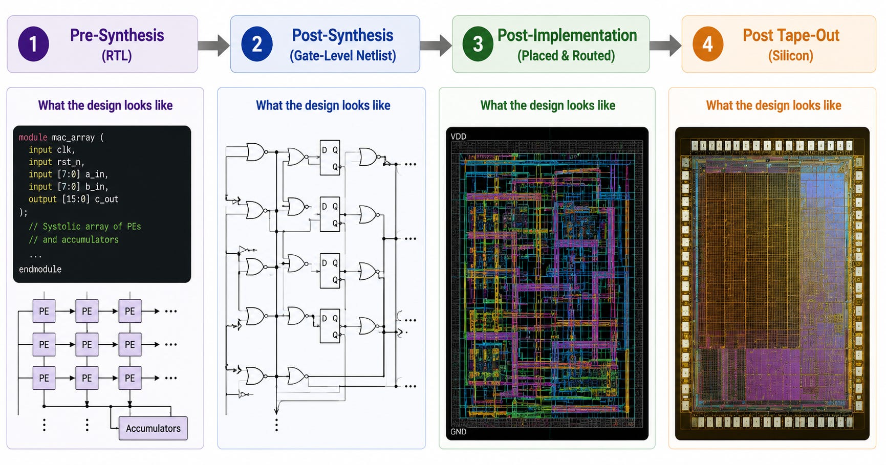
Microarchitecture analysis is most common at the Post-Synthesis and Post-Implementation stage - they are sufficiently accurate, and also provide enough time to make changes to the design before the chip is manufactured. For this post, we’ll focus on post-synthesis results.
Tools and Setup
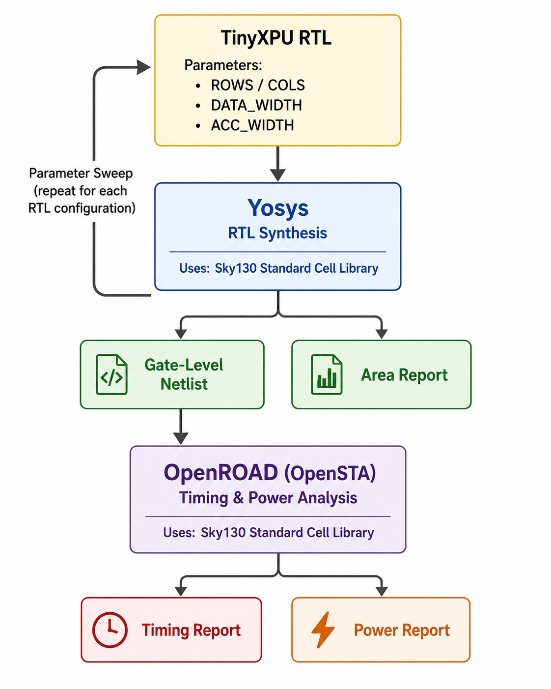
The focus of this post is to explore microarchitecture concepts through the TinyXPU design - so details about the tools are intentionally brief. All the scripts used can be found in the TinyXPU repo.
Our goal was to use an entirely open-source ASIC flow for this analysis - starting with the PDK, for which we picked the Sky130 standard cell library. The RTL was first synthesized with Yosys, which generated the gate-level netlist and provided the area estimates. Then, OpenSTA was used to analyze the synthesized design, extracting both the critical path delay and vectorless power estimates. (The power analysis was available through the OpenSTA engine that ships as part of the OpenROAD project.)
We ran a simple parameter sweep on the design, and parsed the generated logs to get important PPA metrics. Each TinyXPU configuration is defined by three design parameters.
The first is the PE array size (parameter ROWS/COLS), which determines the number of Processing Elements (PEs) arranged in a square systolic array. (So ROWS == COLS) If you are curious about other shapes of systolic arrays, check out this post from min{power}.
The second parameter is the data width (parameter DATA_WIDTH), which determines the precision of the input activations and weights. A larger data width allows the accelerator to represent larger numbers and improve numerical precision, but it comes at a cost, as we will see in this post.
Finally, we vary the accumulator width (parameter ACC_WIDTH), which determines the precision of the partial sums as they propagate through the array. Since each PE performs a multiply-accumulate (MAC) operation every cycle, the accumulator is typically much wider than the inputs to avoid overflow during long accumulation chains.
The Cooking Analogy (Again!)
We said the format is similar to the last post, so how can we continue without the cooking analogy? For the architecture discussion, the focus was: How do we boil eggs efficiently? We experimented with different strategies: boiling one egg at a time, boiling several together, or using multiple burners. Those were architectural decisions.
But when we are talking about microarchitecture, the focus changes to: Can we build a stove that delivers those results within practical constraints? Say we decided to use eight burners to boil more eggs in parallel - would a stove like that fit on the counter-top? And can the kitchen draw enough power to keep all those burners running?
Such references are used sparingly throughout the post to simplify certain concepts, and are displayed as quotes going forward.
Metric 1: Area
Quick Takes
What is it?
Area measures how much space a design occupies on the chip. Larger designs require more transistors, wires, and space between them, which makes the area larger.
In our cooking analogy, this is simply the size of the stove we need for the chosen “egg-boiling” strategy.
Why does it matter?
Smaller chips are cheaper to manufacture, typically consume less power, and can fit in compact electronic equipment.
A compact stove costs less and fits comfortably into a kitchen, while an oversized one may be impractical regardless of how many eggs it boils.
When does it not matter as much?
Quite often these days.
Area is becoming a secondary concern in high-performance datacenter accelerators, where maximizing throughput is more important than minimizing die size and manufacturing costs. Also, you don’t need to stick your H100 GPU on a smartphone or smartglass, so a large area isn’t existential.
In a commercial restaurant, dedicating more floor space to a larger stove may be worthwhile if it allows the kitchen to serve many more customers.
TinyXPU Area Analysis
Area is arguably the easiest PPA metric to build intuition for. Every additional piece of hardware occupies silicon, whether it is another Processing Element, larger multipliers, or bigger registers.
Experiment 1: Area vs. PE Array Size
Our first experiment varies the size of the systolic array while keeping the accumulator width fixed. Each colored line in the plot represents a different data width.
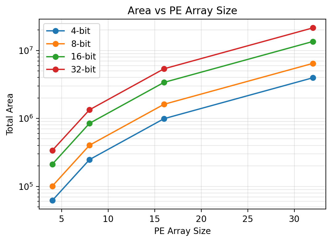
Takeaways: Two clear trends stand out. First, doubling the dimensions of the systolic array roughly quadruples the chip area because the number of Processing Elements also quadruples. Note that the area axis in this plot is logarithmic - so the actual area scales quadratically with the array size. Second, increasing the data width shifts the entire curve upward. Wider inputs require larger multipliers, adders, registers, and interconnect inside every PE, so even with the same array size, the silicon cost increases significantly.
Returning to our cooking analogy, increasing the array size is like adding more burners to the stove, while increasing the data width is like replacing every burner with a larger, more powerful one. Both make the stove more capable, but also larger.
Experiment 2: Area vs. Data Width
Next, we keep the array size fixed (16x16) and vary the precision of the inputs and weights. The accumulator width is also unchanged. (32 bits)
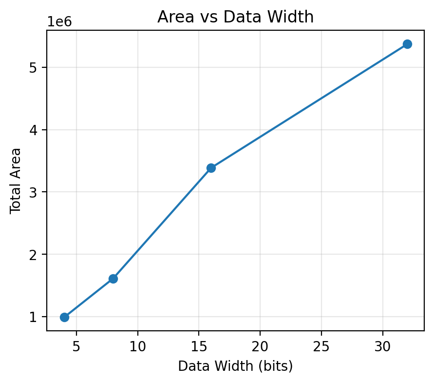
Takeaway: Increasing the data width increases the complexity of every Processing Element. Wider multipliers, adders, and registers all consume additional silicon, so the effect is amplified across the entire array. Although doubling the data width doubles the number of bits, the area does not increase perfectly linearly. The main reason is that arithmetic units, particularly multipliers, become disproportionately larger as operand widths increase. (Interested readers can see the comparison between different multiplier architectures published elsewhere.)
This is one reason why modern AI accelerators often prefer INT8 or even INT4 arithmetic whenever the algorithm can tolerate lower precision - in addition to reducing memory usage, they also reduce the silicon area for each processing element. (In other words, you can pack more processing elements within your chip.)
Experiment 3: Area vs. Accumulator Width
Finally, we fix the array size (16x16) and data precision (8 bits) while varying the accumulator width.
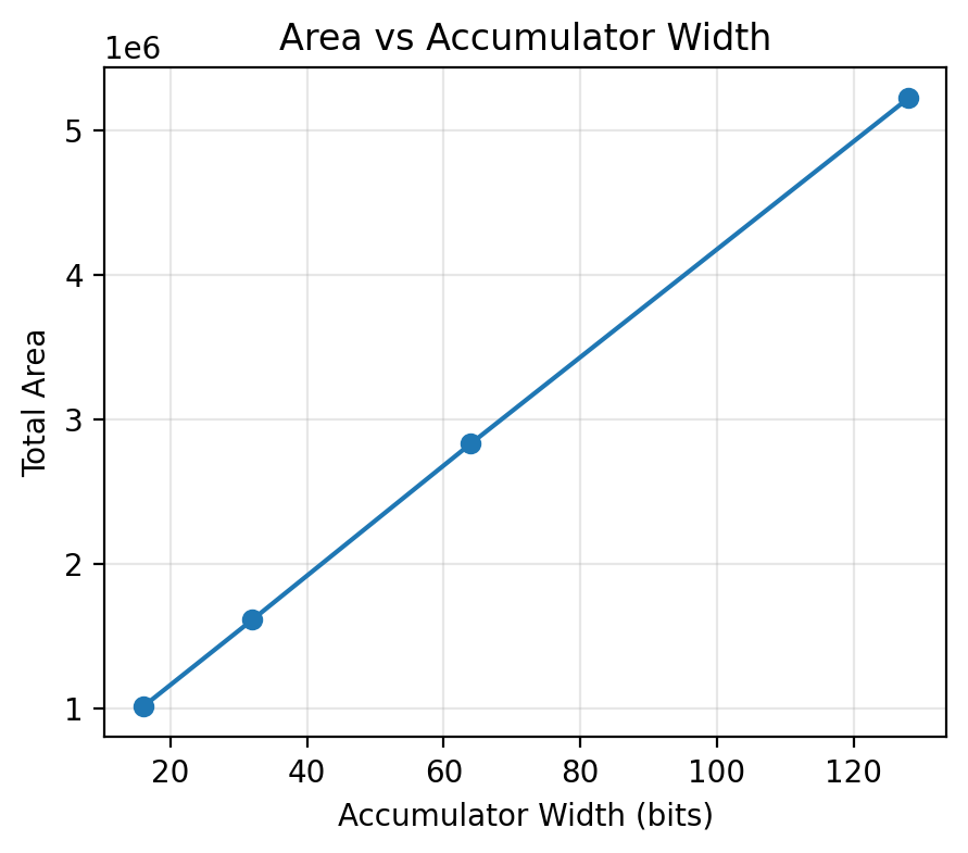
Takeaway: Unlike increasing the data width, increasing the accumulator width produces an almost linear increase in area. The reason is that the accumulator primarily affects the width of the adders and registers that propagate partial sums through the array, both of which scale approximately linearly with the number of bits. (Adders also don’t always scale linearly, but within the range we considered, it seems to stay linear.) To reduce area, the accumulator size should be limited to the numerical range that the workload requires.
For an optimal stove area, make sure that the burners are as big as the pots - anything bigger results in wasted space.
Metric 2: Clock Frequency
Quick Takes
What is it?
Clock frequency is the maximum rate at which a design can reliably execute one clock cycle. It is determined by the longest delay through the hardware. See this Chip Insights post for details:

In our analogy, it is like how quickly the burners can heat the pot, or the rate of gas flow to the burners.
Why does it matter?
A higher clock frequency allows the same hardware to perform more work per second, improving overall performance.
Faster burners boil the eggs sooner.
When does it not matter as much?
If the workload is limited by memory bandwidth, communication, or algorithmic dependencies, increasing the clock frequency may provide little benefit. Essentially, if utilization is low, then increasing the frequency wouldn’t help much.
If you don’t have sufficient eggs ready to be boiled in the first place, then even a faster burner won’t allow you to boil more eggs.
TinyXPU Frequency Analysis
Signals in a chip do not propagate instantaneously. As they pass through multiple logic gates between two flip-flops, each gate introduces a small delay. The longest of these paths, called the critical path, determines the maximum operating frequency of the design. (In other words, the clock period must be at least as long as the time it takes for the signals to propagate through this path.)
Timing analysis is typically performed by targeting a specific frequency (and clock period) and analysing the “slack”, which is the time available (positive slack), or the additional time (negative slack) needed to meet the timing requirements. If the slack is negative, the designer has two options: modify the design to ensure timing is met, or increase the clock period.
For this post, our goal is to simply analyze the clock frequency trends for different TinyXPU configurations. So we picked a clock period of 20ns for all our runs. This resulted in both positive and negative slacks across the runs, but instead of reporting the slack, we extracted the data arrival time of the critical path (the longest combinational path between two sequential elements) and used its reciprocal to estimate the maximum achievable clock frequency.
Experiment 1: Frequency vs Accumulator Width
Fix the data width to 8 bits, and sweep the accumulator width in the 8x8 PE array configuration.
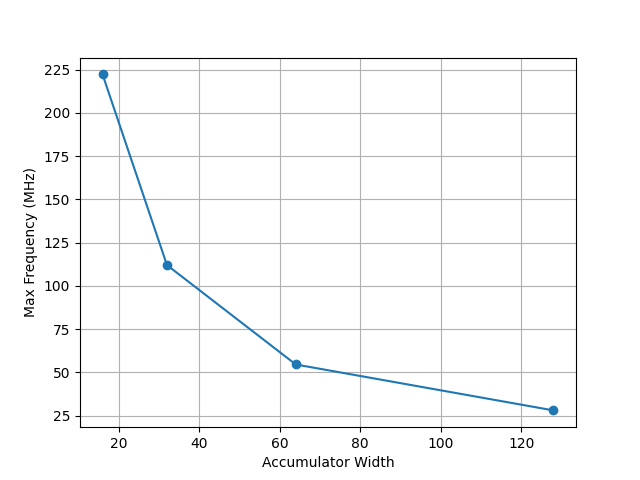
Takeaways: Increasing the accumulator width has a clear impact on clock frequency. Since every multiply is followed by an accumulation, wider accumulators require wider adders on the critical path, increasing the delay through each Processing Element. Unlike the data-width experiment, this trend is almost perfectly linear. Doubling the accumulator width roughly doubles the adder delay, reducing the maximum operating frequency.
The fastest way to boil your egg is to use a small pot on a small burner.
Experiment 2: Frequency vs PE Array Size
Here, we fix the data width to 8 bits, accumulator width to 32 bits, and vary the array size.
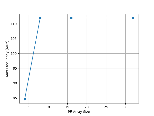
Takeaways: Perhaps the most surprising result is that increasing the array size has almost no impact on the maximum clock frequency. This is expected at the post-synthesis stage, where the critical path is contained almost entirely within a single Processing Element. (The long wires that would connect distant registers in a real chip have not yet been accounted for).
One interesting exception is the 4×4 array, which achieves a noticeably lower maximum frequency than the larger configurations. At first glance, this seems counterintuitive, as the smallest design should be the fastest, right?
We have a theory for why this is happening, but we’ll leave this as a fun exercise. Leave a comment if you can guess what’s causing this behavior.
Experiment 3: Frequency vs Data Width
In this plot, we measure the impact of changing data width by fixing accumulator width to 32 in a 16x16 PE array.
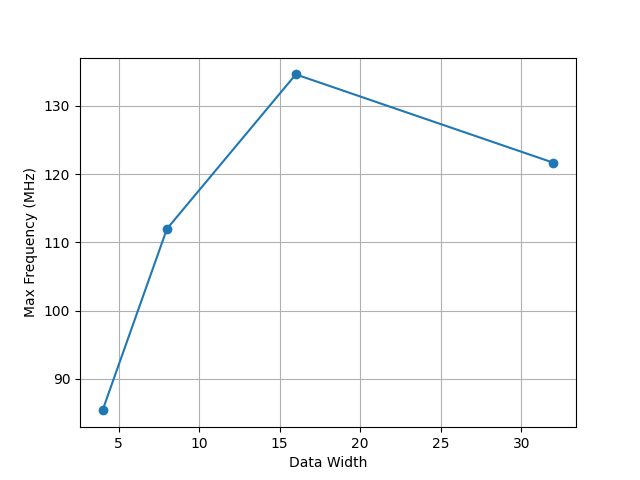
Takeaways: Unlike area, the relationship between data width and maximum operating frequency is not monotonic. Although larger multipliers generally require more hardware, the synthesized critical path depends on the specific gate-level implementation chosen by the synthesis tool. Internally, the tool may restructure arithmetic logic, optimize the multiplier and accumulator differently, select alternate standard cells, or balance the surrounding combinational logic.
In our experiments, changing the operand width altered both the critical path and the logic structure generated by the optimizer. As a result, the 16-bit configuration achieved the highest operating frequency, outperforming both smaller and larger datapaths.
This was the most unexpected result in this study, but we are leaving it here to demonstrate how sensitive microarchitecture analysis could be to the underlying EDA tools and their quirks. We expect that a commercial EDA tool would be better optimized to handle 4 and 8 bit multipliers and result in a more uniform trend.
Metric 3: Power
Quick Takes
What is it?
Power measures the rate at which a chip consumes electrical energy while operating. It includes both the energy spent performing computation and the energy consumed even when parts of the chip are idle. See this Chip Insights post for details about power analysis:
In the kitchen, this is the gas required to keep the stove running.
Why does it matter?
Power determines battery life in mobile devices, electricity costs in datacenters, and how much heat the cooling system must remove.
If you use an extremely power-hungry stove, you will pay more in utility bills.
When does it not matter as much?
It always matters, but may not be existential for new architectures (as they are still experimental and not widely deployed), and performance critical applications - as long as it stays below a certain threshold.
Say you are having people over for the weekend, and you need to boil a lot of eggs, you might not care how much gas the stove consumes.
TinyXPU Power Analysis
To estimate power consumption, each synthesized design was analyzed using OpenROAD’s built-in power analysis. For simplicity, instead of picking a specific workload, the analysis was performed in vectorless mode with a toggle rate of 0.5. This means that, on average, every signal is assumed to have a 50% probability of switching on each clock cycle, providing a rough estimate of dynamic activity across the design. (we explain the limitation of this in an upcoming section.)
Experiment 1: Power vs PE Array Size
With input precision of 8 bits and accumulator width of 32 bits, we look at how power changes for different PE array configurations.
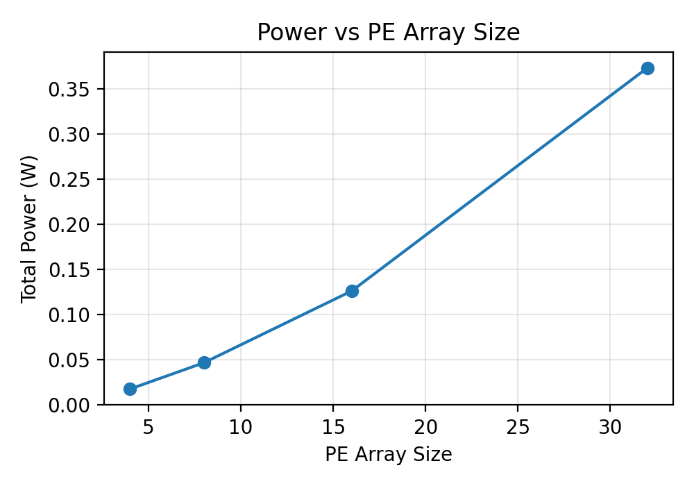
Takeaways: Unlike clock frequency, power increases dramatically as the PE array grows. This is expected because every additional Processing Element introduces another multiplier, accumulator, registers, and routing logic that consume power whenever they switch. The increase is particularly steep because the total number of processing elements grows quadratically with the array dimension. (If you remember, we did exactly this in our architectural analysis post to claim a higher throughput - we are paying the cost now!)
Imagine expanding from a stove with 16 burners to one with 64, then 256, and eventually 1024. Even if each burner consumes the same amount of energy, operating many more of them at once dramatically increases the total power required.
Experiment 2: Power vs Data Width
We vary data width in a 8x8 PE array with 32 bits accumulator width.
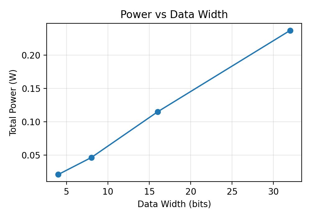
Takeaways: Increasing the data width also raises the total power consumption, although for a different reason. Wider operands require larger multipliers, wider registers, and more combinational logic inside every Processing Element. These additional transistors contribute both more capacitance and more switching activity, increasing the energy consumed on every clock cycle.
Unlike the frequency experiment, which showed an irregular trend due to synthesis optimizations, the power results follow a much more intuitive pattern. Regardless of how the synthesis tool implements the arithmetic, wider datapaths require more hardware and therefore consume more power.
Experiment 3: Power vs Accumulator Width
8 bits of data width, 8x8 PE array configuration.
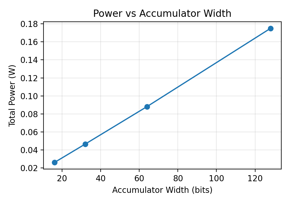
Takeaways: The accumulator width has a similarly predictable effect on power. Wider accumulators require larger adders, wider registers, and additional interconnect, all of which contribute to higher switching capacitance, and hence larger power consumption. As the accumulator width increases, every processing element becomes more expensive to operate, causing the total accelerator power to increase steadily.
This is like replacing every burner with a larger commercial-grade burner. The stove now requires more energy to perform its job, even though the total number of burners remains unchanged.
Analyzing All Metrics Together
Up to this point, we have examined area, frequency, and power independently. In practice, however, hardware architects rarely optimize a single metric in isolation. Instead, they explore a design space, where every point represents a different implementation with its own trade-offs. This plot compares the estimated computational performance of each TinyXPU configuration against its total power consumption. Here, performance is estimated as the product of the number of Processing Elements (PEs) and the maximum operating frequency, and is normalized to the smallest design for easier comparison.
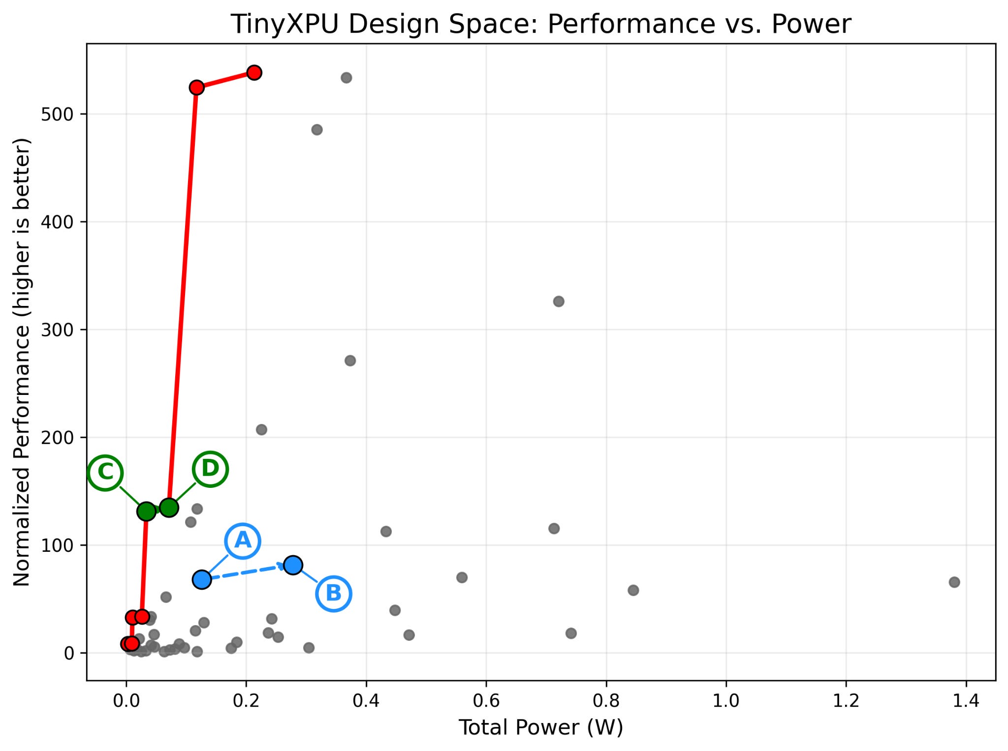
The blue points (A and B) illustrate the concept of a dominated design. Point A corresponds to a 16×16 PE array with an 8-bit data width and a 32-bit accumulator, while point B uses the same array size and accumulator width but increases the data width to 16 bits. Although B consumes significantly more power, it delivers only a modest increase in performance. Since A achieves nearly the same throughput while using less power, B is said to be dominated. More generally, a design is dominated if another configuration provides equal or better performance while consuming equal or less power. Dominated designs are generally discarded because there is always a better alternative.
The red points connected by the red line form the Pareto frontier, representing the set of configurations that are not dominated by any other configuration. Every point on this frontier represents a valid design choice, and moving along the frontier requires trading one metric for another.
The green points (C and D) on the Pareto frontier are interesting. Point C corresponds to a 16×16 PE array with a 4-bit data width and a 16-bit accumulator, while D increases only the data width to 8 bits, keeping the array size and accumulator width unchanged. This change increases the normalized performance by only about 3%, but more than doubles the total power consumption. Although neither design dominates the other, the small performance increase comes at a significant energy cost along this part of the Pareto frontier.
Finally, notice that the Pareto frontier consists of discrete points rather than a smooth curve. Unlike software, hardware parameters such as array dimensions, data width, and accumulator width can only take on a finite number of valid values. We cannot build a 17-bit datapath or a 20×20 systolic array simply because it would lie on a more favorable part of the curve. Instead, hardware architects evaluate a finite set of candidate designs and select the configuration that best balances performance, power, and area for their target application.
Some Practical Considerations
While these results were meant to introduce microarchitectural analysis and highlight some high-level trends, they do not capture many physical effects that appear later in the design flow.
For area, the reported values represent the total area of the synthesized standard cells, not the final chip size after physical implementation. During placement, additional whitespace is introduced to satisfy routing, congestion, clock tree synthesis, and design rule constraints. Consequently, the final die area is typically larger than the synthesized cell area, especially for larger designs where routing becomes more challenging.
For timing, the analysis assumes ideal interconnects. Since the design has not yet been placed and routed, the delays introduced by long wires, clock distribution, and routing parasitics are largely absent. This explains why the maximum operating frequency remains almost independent of the PE array size in our experiments. After place-and-route, these interconnect delays would become a much larger contributor to the critical path, particularly as the array grows.
Finally, the power results should be interpreted as rough estimates rather than accurate measurements. The analysis is vectorless, meaning the EDA tools assume a fixed switching activity instead of using real workload traces. As a result, the reported dynamic power can differ significantly from what would be observed under actual operation. In practice, accurate power analysis requires realistic switching activity (SAIF or VCD files), along with extracted interconnect parasitics after place-and-route. Process-voltage-temperature (PVT) variations and clock tree synthesis also have a significant impact on the final power consumption.
Why does all this matter to an Algorithm Designer?
If you’re an algorithm designer and you’ve made it this far, we hope this final message will make it all worth it.
Architectural ideas are often evaluated using simple models. If doubling the number of processing elements doubles throughput, or increasing the buffer size reduces memory traffic, the idea looks like a clear win. But once someone begins implementing that architecture, physical constraints start to appear.
A larger systolic array requires more wires connecting processing elements, which makes routing more difficult and can reduce the maximum clock frequency. Adding more parallel compute units increases throughput, but it also increases power consumption and can make the chip too large or too expensive to manufacture. Even something as simple as adding another pipeline stage may improve clock frequency while increasing latency. These tradeoffs are invisible at the architectural level, but they become impossible to ignore during microarchitectural design.
This doesn’t mean algorithm designers need to become microarchitects. But keeping one eye on these microarchitectural constraints can lead to better architectural decisions from the very beginning. An algorithm that is designed with area, clock frequency, and power in mind is far more likely to become an efficient hardware implementation.
That is the essence of hardware-software co-design that we aimed to provide through this series of posts. Here are the previous parts:


Subscribe to Chip Insights and min{power} for more and let us know if there is something else you would like us to explore.
Hello, my name is Hosein Aslami. I’m a graphic designer, and I’m very passionate about graphic design and creative work. Would it be possible for me to work with you? I would be happy to show you my skills and experience through a project. Thank you for considering me.
I’m passionate about 3D modeling, and I would love the opportunity to work with you. I have extensive experience in 3D modeling and graphic design, and I’m confident in my skills. I would be happy to take on a test project to demonstrate my abilities.