
Mapping Algorithms to Custom Silicon - Part 2
Running matrix multiplication on a TPU-style architecture


Disclaimer: Opinions shared in this, and all my posts are mine, and mine alone. They do not reflect the views of my employer(s) and are not investment advice.
This post is the second in our series on custom hardware accelerators. In part 1, we introduced the hardware-software interface problem that has kept the two domains as separate islands and limited co-innovation. We also introduced two approaches to overcome this gap. If you haven’t done so already, check out that post here:

In this part, we present TinyXPU, an open-source, extensible project we are building in conjunction with this series of posts. In this post, we focus on two pieces:
The hardware architecture of TinyXPU
The software interface that allows it to run ONNX models
The goal of this project is to show what the bridge between software and hardware looks like in practice, and is a stepping stone to the architectural analysis we have planned in upcoming posts.
Why Matrix Multiplication
The first important decision is to pick the right algorithm to study. We picked Matrix Multiplication, primarily because of its widespread use in many of today’s most important software domains. Here are a few representative examples:
Deep Learning: Neural network layers compute weighted sums using matrix multiplications.
Robotics: BLAS, in particular the Level 3 GEMM routine, is used in many robotics libraries
Computer Graphics: Shaders use matrix math for transformations; modern APIs like Vulkan have started exposing this directly.
Matrix multiplication also stresses both compute throughput (number of arithmetic operations completed per second) and memory bandwidth (the number of bits read from memory per second). This helps us identify both compute and memory bottlenecks - a topic we will explore in future posts.
Why build an accelerator from scratch
We are not the first to focus on matrix multiplication, and we certainly won’t be the last. As mentioned in an earlier post, there has been an explosion of “processing units” like TPUs and NPUs that, at their core, accelerate matrix multiplication. In fact, modern GPUs and even CPUs now support matrix multiplication extensions and dedicated units to handle the operation efficiently. There are also a number of “tinyTPU” projects out there with an architecture very similar to the one we will be demonstrating. (Some examples are tiny-tpu-v2/tiny-tpu and Alanma23/tinytinyTPU.) So before we go any further, we wanted to explain why we are doing this from scratch.
Our main motivation is that building from scratch allows us to understand (and hopefully explain) everything we are doing from first principles. As you will see, we are only starting with two simple SystemVerilog files. This way, we do not have to make any assumptions or shoot in the dark to understand architectural decisions. This also allows us the flexibility to scale or modify the architecture for future posts in this series.
It’s not just the hardware architecture that could be confusing. As we mentioned in Part 1, the software interface is messy and still evolving. As this is the first implementation in our series, we wanted to keep a simple but still operational software interface. Setting up this interface is important to obtain performance metrics that will be used for architectural analysis in future posts in this series.
With that motivation, we can now look at the two parts of the TinyXPU project: the hardware architecture and the software interface.
The Hardware Architecture
We built the first version of our matrix multiplication accelerator based on the weight stationary systolic array architecture: the same one at the heart of Google’s TPUs. While this post will not go into the details of this architecture, here’s a dedicated post that’s got you covered:

The Processing Element (PE)
The core block in TinyXPU is called a Processing Element (PE), a term that originated in H. T. Kung’s seminal work in 1982. Here’s the block diagram of our PE (the SystemVerilog implementation can be found in pe.sv):
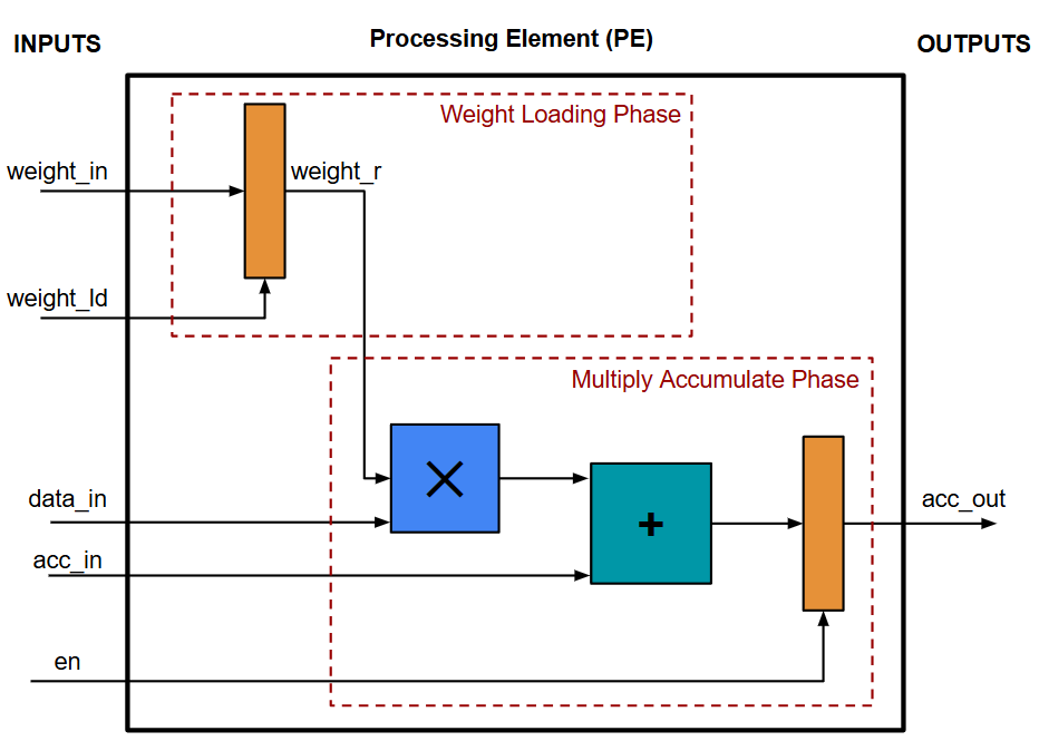
This PE block executes the following operation:
acc_out = data_in * weight_in + acc_inHowever, this operation is executed in two phases:
Weight Loading Phase: In this phase, the value of weight_in is stored in the register weight_r when weight_ld is set to 1.
Multiply Accumulate Phase: Here, the stored value weight_r is multiplied with data_in, and acc_in is added to get the final result. When en is set to 1, this result is sent as the output.
The reason for having these two phases comes from its primary use case in neural networks, where we typically process multiple inputs (called “batches”) using the same weights - so loading the weights once prevents the need to continuously broadcast its value during the computation. This is called a "weight-stationary" architecture, indicating that the weights don't move through the array in the Multiply Accumulate Phase.
It’s also important to highlight that the Multiply Accumulate Phase has a latency of 1 cycle - which means that the output of the PE is ready one cycle after the inputs. This pipeline stage is needed to break the combinational logic path when two PEs are connected together, in order to achieve a high clock frequency. (If you are new to digital design, this post on Static Timing Analysis would help you understand why this matters.)
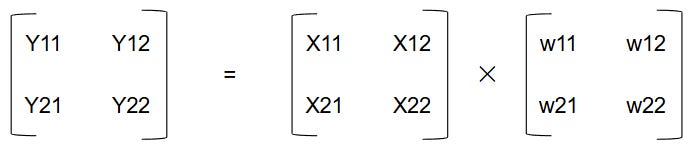
Matrix Multiplication on a PE array
The functionality of a single PE can be achieved using the Arithmetic and Logic Unit (ALU) in most CPUs. So, to really understand the benefit of a PE array, let’s consider a PE array with 2 rows and 2 columns, and map a matrix operation on it. Specifically, we will be implementing this operation:
Our PE array performs matrix multiplication by arranging PEs in a grid where data flows between neighboring elements. Each PE stores one weight value and performs a multiply-accumulate operation every cycle. As input values move across the array, partial sums are passed between PEs until the final output values emerge from the last column. We depict the cycle-by-cycle dataflow in this diagram:
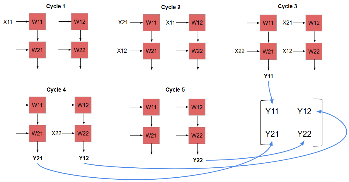
In the first cycle, X11 is passed as input to PE with weight W11
In the second cycle, X11 moves on to the next PE. (with weight W12.) Simultaneously, X21 and X12 are passed to the first PE column. (with weights W11 and W21.)
In the third cycle, X21 and X12 move to the second PE column.( with weights W12 and W22.) Also, X22 is passed to PE with weight W21. In this cycle, we also have the first output value ready:
Y11 = X11 × W11 + X12 × W21Note that the latency (time from first input to first output) is 2 cycles in this example. As the number of rows of the PE array increases, this latency also increases. After the first output, new outputs are ready in every adjacent cycle, as we will see.
In cycle 4, X22 moves to the second PE column. We also get output Y21 and Y12 from both the PE columns.
Finally, in cycle 5, the last output Y22 is ready in the second PE column.
What makes this an accelerator?
The biggest advantage of this PE architecture is that we read the operands only once from memory. In the above example:
Weights W11, W12, W21, W22 are only read in the Weight Loading Phase and are then stored in the PEs
Although Inputs X11, X12, X21, X22 are used twice during the matrix multiplication, they are only read once (For example, after X11 is read in Cycle 1, it is just passed to the next PE in Cycle 2 - it does not have to be read again.)
In a standard CPU, the intermediate values would need to be stored somewhere. It could be stored in a fast register for small matrices, but might need to spill to slower caches and main memory as the matrix size increases.
Our PE array avoids repeatedly fetching operands from memory because values propagate directly between neighboring PEs. This is what makes the PE array architecture great for matrix multiplication. (This statement assumes PE array size and matrix sizes are the same - the PE array SystemVerilog implementation in TinyXPU is parametrized to support different number of rows and columns. In our upcoming posts, we will explore the impact of these different configurations on the performance of our chip.)
Finally, although our current implementation is just a PE array, we want to highlight that a real accelerator has other components in its microarchitecture which we are skipping here for the sake of simplicity:
We need to define an Instruction Set Architecture (ISA) and include an instruction decode unit
We need a Unified Buffer (typically SRAM) to hold the matrix data before streaming it into the PE array. (Typically, a DMA controller would stream data from CPU DRAM to the local SRAM.)
As this project evolves, some of these components will be (and must be) included in the design.
The Software Bridge
In the previous section, we described the hardware implementation of our TinyXPU Matrix Multiplier. Hopefully, you are convinced that the PE array is an improvement over using general-purpose CPUs for matrix multiplication. If you are a hardware engineer, many of your projects stop here with this question: how do you connect your hardware with the existing software ecosystem and actually run matrix multiplication on your chip? In part 1, we described two approaches to solve this problem - Runtime-level and Compiler level integration. In this section, we will implement runtime-level integration using an ONNX Runtime Execution Provider.
The ONNX Runtime Flow
The flow used in our project is intentionally simple.
First, a small ONNX model containing a matrix multiplication operation is generated using a Python script. An ONNX model represents a computation as a graph, where each node corresponds to an operation such as matrix multiplication. In our implementation, the generated ONNX file includes a MatMulInteger operator, as shown in this code snippet:
X = helper.make_tensor_value_info("X", TensorProto.INT8, [None, W_data.shape[0]])
Y = helper.make_tensor_value_info("Y", TensorProto.INT32, [None, W_data.shape[1]])
W_init = numpy_helper.from_array(W_data, name="W")
node = helper.make_node("MatMulInteger", inputs=["X", "W"], outputs=["Y"])
graph = helper.make_graph(
[node],
"MatMulInteger_4x4",
[X],
[Y],
initializer=[W_init],
)
Next, a Python driver loads this model using ONNX Runtime and registers the TinyXPU Execution Provider (EP), as shown in this code snippet:
ort.register_execution_provider_library("SampleEP", path_to_dll)
session_options = ort.SessionOptions()
session_options.add_provider_for_devices(tinyxpu_devices, {})
The goal of the EP is to inspect the ONNX model, looking for an eligible operation: in our case, it would be MatMulInteger. (See the GetCapabilityImpl() method in the TinyXPU EP for details.) The ONNX Runtime will call the function where we registered our ability to execute MatMulInteger when the session is instantiated.
When the runtime encounters the matrix multiplication operation, it dispatches that operation to the TinyXPU backend (via the ComputeImpl() hook) instead of executing it on the CPU (which is the default option when no match is found.) This way, we are able to connect the TinyXPU hardware directly to software without requiring a custom compiler - a major benefit of this approach.
Practical Constraints
Much like the hardware implementation, our current ONNX interface has some constraints that we would like to highlight.
Firstly, instead of exporting a Pytorch/Tensorflow implementation into the ONNX format, we directly use a Python script to generate an ONNX model containing a single MatMulInteger operation. This keeps the software stack minimal while still exercising the same ONNX Runtime execution flow that would be used with real models. Pytorch and Tensorflow both support functions to export to ONNX, so this additional step is fairly trivial. In fact, ONNX is a common intermediate exchange format before going to many hardware APIs including TensorRT for NVIDIA embedded devices, Qualcomm Hexagon, and others.
As mentioned in the previous section, we do not yet have an FPGA or ASIC implementation of our design for this part. That’s where Verilator comes into the picture. The SystemVerilog implementation of the TinyXPU systolic array is compiled into a cycle-accurate C++ model using Verilator. The TinyXPU Execution Provider links directly against this generated C++ model. When ONNX Runtime dispatches a matrix multiplication operation (MatMulInteger) to TinyXPU, the Execution Provider performs three steps (See the ComputeImpl() method in the TinyXPU EP for details):
Read input tensors from ONNX Runtime
Drive the Verilator simulation input signals and toggle the clock
Collect output signals from the simulation
So, in our implementation, the ONNX runtime connects the software world with a cycle-accurate simulation of the hardware, as shown in this diagram below (The “real silicon” version of this diagram was included in part 1):
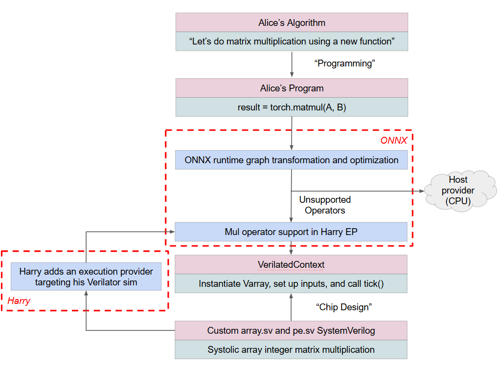
It’s important to mention that irrespective of whether we are running on a Verilator-generated simulation, custom hardware implemented on FPGAs or as an ASIC, or existing processors on an SoC like CPUs, GPUs, or NPUs - this implementation successfully abstracts the hardware away from the software - our stated goal from Part 1.
Part 2 ends here. Although the current implementation is intentionally minimal, it already gives us a complete system: a software stack capable of dispatching matrix multiplication operations to a cycle-accurate simulation of our accelerator. This demonstrates how runtime-level integration works, and more importantly, provides a useful platform for experimentation.
In the next post, we use this framework to analyze the architecture in more detail, exploring how design parameters such as the size of the array compared to the workload and memory bandwidth affect throughput, latency and utilization. Check it out here:

The TinyXPU project will also expand to support activation functions to run complete ONNX ML models that can be deployed on an FPGA. To get notified about all this and more, subscribe to both Chip Insights and Min{power}. And if you have some experience taking up similar projects, or have an interesting direction for us to explore, let us know in the comments.
 | A guest post by
|
Great work guys.. super useful to understand from the ground up.